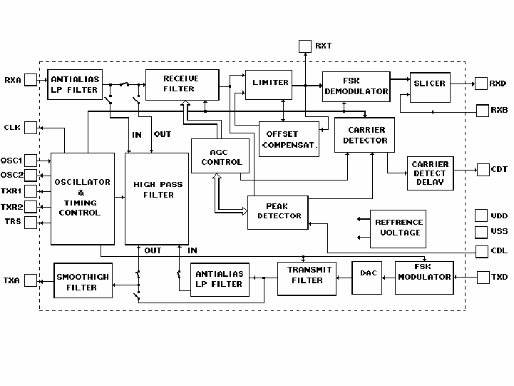
The TCM3105 modem is made up of four functional blocks:
Transmitter
The transmitter comprises a phase coherent FSK modulalor, transmit filter and transmit amplifier (fig 3). The modulator is a programmable frequency synthesiser which derives the output frequencies by variable division of the 4.4336 MHZ Master Clock Frequency. The division ratio is set by the state of the transmit receive standard pin (TRS). The transmit bit rate pins (TXR1 and TXR2) and the data input (TXD).
The frequencies are given in fig. 6 and the data convention is "1" equals mark and "0" equals space.The final stage of the Transmitter section is the Transmit filter followed by the Transmit amplifier.
TRANSMITTER
The frequency response of the transmit filter is dependent upon the mode selected on the TRS, TXR1, TXR2 inputs. In all modes, the first filter section is a switched capacitor low-pass filter which limits the level of harmonics at its output. (This filter has a switching frequency response which provides optimum characteristics for each transmit frequency). For the 75 150 bauds receive mode and 600 1200 bauds transmit mode, the output of the switched capacitor low-pass filter is applied in turn, to an antialiasing filter, a switched capacitor high-pass filter and equaliser before passing through a smoothing filter, the output of which is the TXA pin. This suppresses receive band frequencies such that they do not appear at TXA.
For the 600 1200 bauds receive mode, the output of the switched capacitor low-pass filter is applied to a continous low-pass filter, in order to remove harmonics due to sampling, before outputting the signal on TXA.
receiver
The demodulation function of the receiver is based on the principle of frequency to voltage conversion. The receive section is shown in fig.4 and comprises an antialiasing prefilter, a receive amplifier, group delay equaliser, receive filter, limiter, demodulator, post-demodulator filter and slicer. The receive standard is set by the state of the TRS, TXR1 and TXR2 input.
The antialiasing prefilter is a continuous low-pass filter which prevents aliasing, due to the sampling nature of the receive filter and group delay equaliser, of high frequency components of the input signal at RXA.
The receive amplifier is of variable gain and its purpose is to maintain a suitable signal output level from the receive filter across the dynamic range of the input signal at RXA.
The receive filter is designed to limit the bandwidth of the signal presented to the demodulator, reducing out of band interference and also giving high rejection of backward channel frequencies which are typically present at much higher levels than the received signal.
The receive filter achieves this by taking the form of a single band-pass stage when in 5 75 150 bauds receive mode, but in the 600 1200 bauds receive mode an additional high-pass filter stage is placed ahead of it, thereby limiting the effect of the frequencies corresponding to the lower bit rates.
RECEIVER
The Group Delay Equalizer is a switched capacitor network which corrects for both phase and attenuation distortion introduced by the line and receive filter. The output from the Group Delay Equalizer is measured in order both to feedback to the receive amplifier for automatic gain control and to control the carrier detect flag (CDT).
The limiter then converts this analogue signal into a squared FSK modulated signal which is then presented to the demodulator.
The demodulator, which is an edge triggered multivibrator, performs the frequency to voltage conversion which allows to extract the transmitted data from the modulated signal. The monostable triggers on both the positive and negative going edge of the limited signal, thus producing at its output, a stream of fixed lenght pulses at a frequency which is double that ot the limited input signal.
The dc component of this signal is inversely proportional to the received frequency and is extracted by a switched capacitor, low-pass, post demodulator filter.
The output analogue signal of the post demodulator filter must be converted into a binary signal by the slicer.
This is performed by a comparator whose reference and therefore decision threshold is externally set, by input, to the midpoint of the analogue signal. (The midpoint is defined as that level between the dc output level of a continuous mark frequency and the dc output level of a continuous space frequency).
This external adjustment on RXB also balances possible internal offsets. (for RXB adjustment procedure see page 4-15).
The output of the comparator is then available at the RXD output.
carrier detector
The carrier detect circuitry comprises an energy detector and digital delay. The energy detector and digital delay. The energy detector compares the total signal level at the output of the receive filter to an externally set threshold on the CDL pin. If there is a loss of carrier singal then CDT (carrier status flag) will not go low during a time delay fixed by the digital delay.
If, however this fixed time has elapsed and the carrier is still not present then CDT goes low and "carrier fail" is indicated.
The carrier detector also has a minimum 2 dbm hysteresis to avoid oscillations on CDT when the receive level is close to the carrier detect threshold.
timing and control
An on-chip oscillator runs from an external 4.4336 MHz PAL crystal connected between OSC1 and OSC2 or an external signal driving OSC1. A clock signal equal to 16 times the highest selected bit rate (transmit or receive) is available on the CSK pin.
The single supply implies that all analogue functions be referenced to an internally generated voltage. All analogue inputs and outputs must be a.c. coupled. or d.c. bias must be adapted.
